Materials and Manufacturing
Materials and manufacturing deal with the application of knowledge relating to the composition, structure and processing of materials to their properties and performance in applications.
Over the past two decades, there has been significant progress in the use of composite materials in a range of everyday applications that require materials with superior performance characteristics. Composite materials are engineered materials that are made from two or more constituent materials with significantly different physical or chemical properties. Nanotechnology has emerged as a key technology used in fabrication of new classes of composite materials with vastly improved properties and performance.
Though “top-down” fabrication methods are still used, nanotechnology has empowered a “bottom-up” approach to modify the material properties at the nanoscale level.
A classic (“top down”) method for nanofabrication is electron beam lithography (EBL). In EBL a beam of electrons is scanned across a surface covered with a film (called the resist). The beam removes selectively either exposed or unexposed regions of the resist. This process results in very small structures in the resist that can be lithographically transferred to another material and used to create very small electronic devices. EBL can produce structures smaller than 10 nm which can be used in applications such as solar cells and other semiconductor and optoelectronics devices.
Another example of a method for the fabrication of nanopatterns is called nano-imprint lithography. This is a tool in which a master mold is made using a serial technique like EBL, and this mold is stamped into soft polymer like polydimethylsiloxane (PDMS). This method has achieved resolutions of 10 nm and can be used to make microchannels for biomedical devices and small scale chemical reactors.
An interesting method of forming a periodic nanostructure from the bottom up is called self-assembly. Self-assembly occurs when certain atoms, molecules or other nanoscale structures are energetically attracted to one another and come together to form a repeating pattern on the molecular level. This technique can be likened to a jigsaw puzzle that assembles itself after its pieces have been jumbled together in a box. Can you imagine that happening?
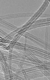
A good example of manufacturing a specific nanostructure through self-assembly is provided by carbon nanotubes (CNTs). CNTs have excellent mechanical, electrical and optical properties. Depending on their use, CNTs can be manufactured to have high tensile strength and high electrical conductivity.
They have been recently used to reinforce and impart mechanical strength to a variety of polymer composites which are used as body armor, transmission line cables and textiles. Ballistic electron transport properties make CNTs an attractive material for device interconnections in computers and for liquid crystal displays (LCDs).
Carbon nanotubes were first synthesized by the Japanese physicist Sumio Iijima when studying the deposits left during the arc-evaporation synthesis of fullerenes (a fullerene is a type of carbon molecule). Since this discovery, carbon nanotubes have been synthesized by controlling the conditions of the arc-evaporation process. Aside from this synthesis method, carbon nanotubes can be fabricated using techniques such as sputtering, chemical vapor deposition, and plasma enhanced chemical vapor deposition. In each of these processing techniques, carbon atoms come together and automatically assemble into the geometry of a carbon nanotube.
Ceramic materials also can be nanostructured and, in some cases, exhibit aspects of self-assembly under certain processing conditions. Generally, ceramics are processed at high temperatures and are often used in applications that require materials that can survive extreme environments.

Image Credit: NASA Ames Center for Nanotechnology
While various ceramics have been used for millennia as building materials (such as bricks and stone blocks), advances in ceramic manufacturing technologies have led to the development of new technical ceramics. These materials serve in a range of modern applications ranging from microelectronics to kitchen appliances. For example, these materials are used in high voltage insulators and as highly insulating materials for space-based probes owing to their excellent thermal and electrical properties. Nanostructured glass-ceramic composites are also used in optical equipment. Overall, materials and manufacturing technologies exploit our understanding of material science to produce state-of-the-art nanostructured materials and related devices with low manufacturing costs and high performance characteristics.


